Understanding Transistors: Structure, Types, and Functionality
Fundamentals and Composition of Transistors
Basic Concept and Role of a Transistor
A transistor is a compact semiconductor device designed to regulate electrical signals by either allowing or blocking current flow. It primarily functions as a switch or an amplifier, enabling control over electronic circuits by modulating signal strength or current passage.
Invented in 1947 by physicists John Bardeen, Walter Brattain, and William Shockley, transistors have become indispensable components in modern electronics, forming the backbone of countless devices.
Structural Elements of a Transistor
Typically, a transistor consists of three semiconductor layers forming three terminals that interface with external circuits. These terminals are:
Base: Acts as the control terminal to activate the transistor.
Collector: The terminal that collects carriers, usually positive in polarity.
Emitter: The terminal that emits carriers, generally negative.
The transistor’s operation hinges on controlling current flow between two terminals by applying a voltage or current at the third terminal.
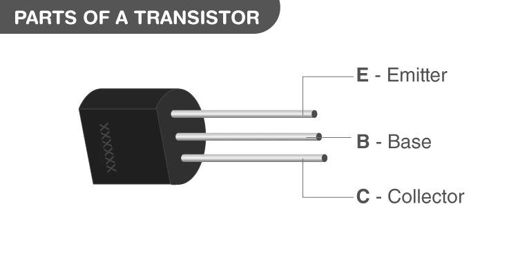
Illustration of transistor terminals and their roles
Example: Identifying Transistor Terminals
In a transistor circuit, if a small current is applied to the base terminal, which terminal controls the main current flow?
Solution: The base terminal controls the transistor’s operation. A small current at the base regulates a larger current flowing between the collector and emitter terminals, effectively switching or amplifying the signal.
Classification and Configurations of Transistors
Primary Types of Transistors
Transistors are mainly categorized based on their construction and operation into two types:
Bipolar Junction Transistor (BJT): Utilizes both electron and hole charge carriers.
Field Effect Transistor (FET): Operates using voltage to control current flow via an electric field.
Bipolar Junction Transistor (BJT) Varieties
BJTs have three terminals: base, emitter, and collector. A small current at the base controls a larger current between collector and emitter. BJTs come in two forms:
PNP Transistor: Consists of an n-type layer sandwiched between two p-type layers. It controls current flow through two series-connected crystal diodes: collector-base and emitter-base.
NPN Transistor: Features a p-type layer between two n-type layers. It is widely used to amplify weak signals by allowing electrons to flow from emitter to collector.
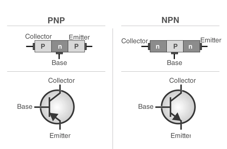
Comparison of NPN and PNP transistor structures
Common Transistor Configurations
Transistors can be connected in three standard configurations, each defining which terminal is common to both input and output:
Common Base (CB): Base terminal is shared between input and output.
Common Collector (CC): Collector terminal is common to input and output.
Common Emitter (CE): Emitter terminal is common to input and output.
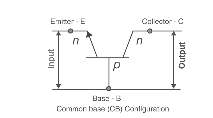
Common Base (CB) transistor configuration
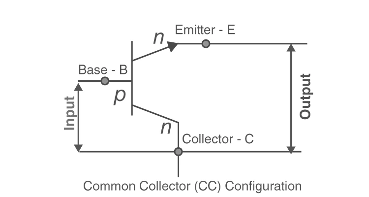
Common Collector (CC) transistor configuration
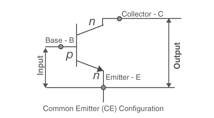
Common Emitter (CE) transistor configuration
Field Effect Transistor (FET) Overview
FETs have three terminals: gate, source, and drain. The voltage applied at the gate controls the current flowing between source and drain. FETs are unipolar devices and are commonly used in low-noise amplifiers, buffers, and analog switches.
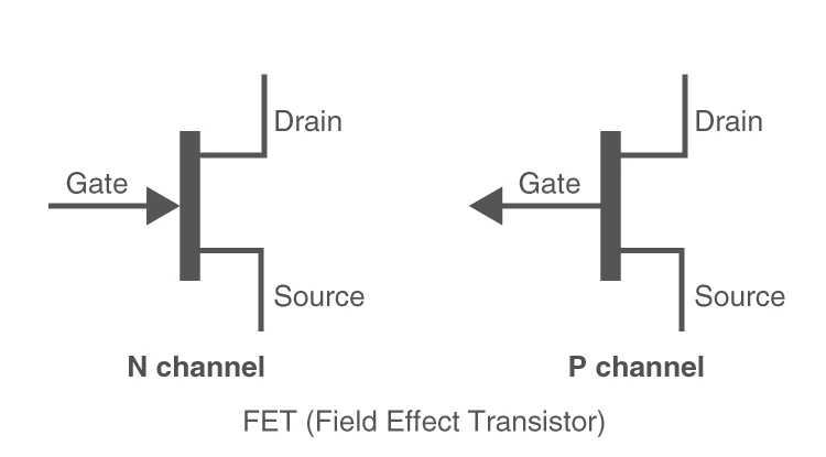
Structure and terminals of a Field Effect Transistor (FET)
Example: Identifying Transistor Configuration
A transistor circuit has the emitter terminal connected to both input and output. Which configuration is this?
Solution: This is a Common Emitter (CE) configuration, where the emitter terminal serves as the common point for input and output circuits, widely used for amplification purposes.
Operational Principles and Performance Characteristics
How Transistors Function
In a Bipolar Junction Transistor (BJT), two P-N junctions exist: one between emitter and base, and another between collector and base. The base-emitter junction is forward-biased, allowing current flow, while the base-collector junction is reverse-biased.
A small current entering the base-emitter junction controls a much larger current flowing from emitter to collector, enabling amplification or switching.
Working of an NPN Transistor
The emitter in an NPN transistor is made of n-type material, rich in electrons. When forward-biased, electrons move from emitter to base, where only a few recombine due to the thin, lightly doped base. Most electrons cross into the collector, allowing current flow despite the reverse bias at the collector-base junction.
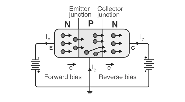
Electron movement in an NPN transistor during operation
Example: Current Control in NPN Transistor
In an NPN transistor, if the base current is increased from 20 µA to 40 µA, and the current gain (β) is 100, calculate the change in collector current.
Solution:
The collector current \( I_C \) is related to base current \( I_B \) by \( I_C = \beta I_B \).
Initial collector current: \( I_{C1} = 100 \times 20 \times 10^{-6} = 2 \times 10^{-3} \text{A} = 2 \text{mA} \).
Final collector current: \( I_{C2} = 100 \times 40 \times 10^{-6} = 4 \times 10^{-3} \text{A} = 4 \text{mA} \).
Change in collector current: \( \Delta I_C = I_{C2} - I_{C1} = 2 \text{mA} \).
Characteristic Curves of Transistors
Transistor characteristics describe how current and voltage relate under different configurations:
Input Characteristics: Variation of input current with input voltage at constant output voltage.
Output Characteristics: Variation of output current with output voltage at constant input current.
Current Transfer Characteristics: Relationship between output and input currents at constant voltage.
Input Characteristics in Common Base Configuration
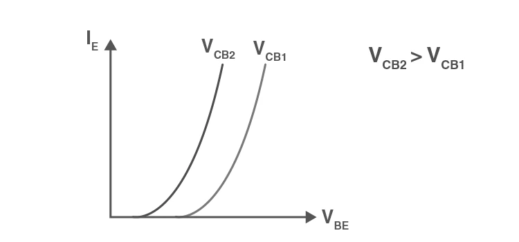
Input characteristic curve for Common Base (CB) setup
Output Characteristics in Common Emitter Configuration
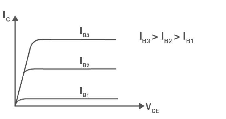
Output characteristic curve for Common Emitter (CE) setup
Current Transfer Characteristics in Common Emitter Configuration
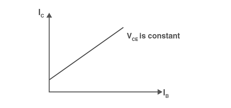
Current transfer characteristic for Common Emitter (CE) configuration
Example: Interpreting Characteristic Curves
In a common emitter transistor, if the base current is held constant and the collector-emitter voltage increases, what happens to the collector current?
Solution: The collector current initially rises with increasing voltage and then saturates, indicating the transistor is in active mode. Beyond a certain voltage, the current remains nearly constant, showing transistor amplification behavior.
Benefits and Constraints of Transistor Technology
Advantages of Using Transistors
Compact size and cost-effective manufacturing.
Low mechanical sensitivity, making them durable.
Operate at low voltages, enhancing safety and efficiency.
Long operational lifespan without significant degradation.
Negligible power consumption in switching applications.
Rapid switching speeds suitable for high-frequency circuits.
Enable development of efficient and complex integrated circuits.
Limitations and Challenges
Lower electron mobility compared to some other semiconductor devices.
Susceptible to damage from electrical surges and thermal stress, such as electrostatic discharge.
Performance can be affected by cosmic radiation and environmental factors.
Example: Evaluating Transistor Suitability
Why might a transistor be preferred over a vacuum tube in modern electronic circuits?
Solution:
Transistors are smaller and more durable.
They consume less power and operate at lower voltages.
They switch faster and have longer lifespans.
Transistors are more cost-effective and suitable for integration.
Quick Reference: Transistor Essentials
Aspect | Details |
|---|---|
Inventors | John Bardeen, Walter Brattain, William Shockley (1947) |
Terminals | Base, Collector, Emitter (BJT); Gate, Source, Drain (FET) |
Primary Types | BJT (NPN, PNP), FET (N-channel, P-channel) |
Common Configurations | Common Base, Common Collector, Common Emitter |
Function | Switching and Amplification of electronic signals |
Advantages | Small size, low power, fast switching, long life |
Limitations | Susceptible to damage, limited electron mobility |
Characteristic Curves | Input, Output, Current Transfer |
Operation Principle | Small base current controls larger collector current (BJT) |
Applications | Amplifiers, switches, integrated circuits |
Glossary of Key Terms
Term | Definition |
|---|---|
Base | The control terminal of a transistor that regulates current flow. |
Collector | The terminal that collects charge carriers in a transistor. |
Emitter | The terminal that emits charge carriers into the base region. |
Bipolar Junction Transistor (BJT) | A transistor type using both electrons and holes as charge carriers. |
Field Effect Transistor (FET) | A transistor controlled by voltage applied to the gate terminal. |
Forward Bias | Condition where a P-N junction allows current flow. |
Reverse Bias | Condition where a P-N junction blocks current flow. |
Current Gain (β) | Ratio of collector current to base current in a BJT. |
Depletion Region | Area around a P-N junction depleted of free charge carriers. |
Common Emitter Configuration | Transistor setup where emitter is common to input and output. |
Frequently Asked Questions
Which transistor terminal is lightly doped and why?
The base terminal is lightly doped to allow most charge carriers to pass through without recombining, enabling efficient transistor operation.
How does the emitter differ from the collector in doping?
The emitter is heavily doped to inject a large number of charge carriers, while the collector is moderately doped to collect carriers efficiently without excessive recombination.
What is the typical biasing arrangement of transistor junctions?
The emitter-base junction is forward-biased to allow current flow, and the collector-base junction is reverse-biased to control the current flow through the transistor.
How many depletion regions are present in a transistor?
A transistor contains two depletion regions: one at the emitter-base junction and another at the collector-base junction.
What is the main function of a transistor in electronic circuits?
Transistors primarily act as switches or amplifiers, controlling the flow and strength of electrical signals within circuits.