CLASS 12-PCB . PHYSICS . PHYSICS PART II . SEMICONDUCTOR ELECTRONICS-MATERIALS-DEVICES-AND-SIMPLE-CIRCUITS
Chapter 6 : Semiconductor Electronics: Materials, Devices And Simple Circuits
Ch 6
PHYSICS
CLASS 12-PCB
Energy Bands and Types of Semiconductor
Energy Bands Explanation
Energy bands are ranges of energy levels that electrons can occupy in crystalline solids. These bands arise due to the close spacing of energy levels in solids, forming continuous bands rather than discrete levels.
There are three important energy bands in solids:
- Valence Band: The band filled with electrons that are bound to atoms.
- Conduction Band: The band where electrons are free to move and conduct electricity.
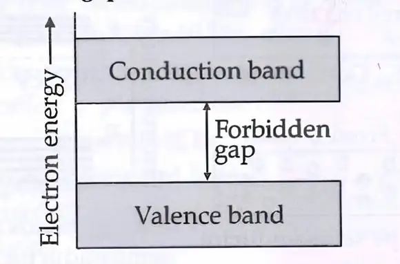
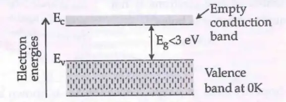
- Forbidden Band (Energy Gap): The energy gap between the valence band and conduction band where no electron states exist.
The size of the energy gap determines the electrical conductivity of the material.
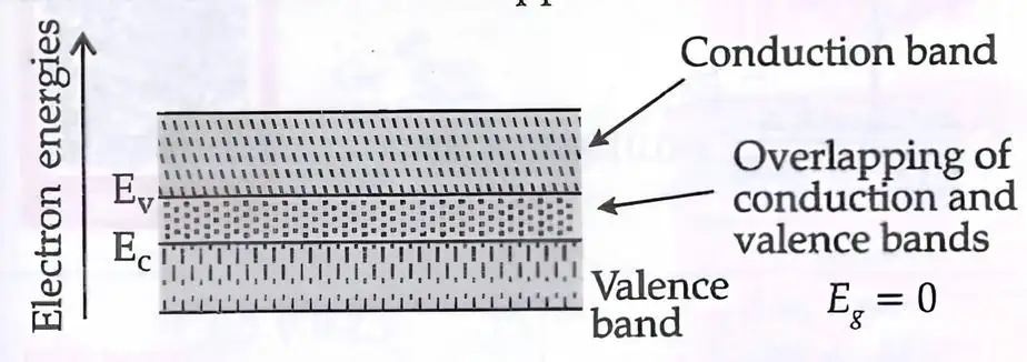
Energy Bands in Different Materials
Conductors: The valence band and conduction band overlap, allowing electrons to move freely and conduct electricity easily.
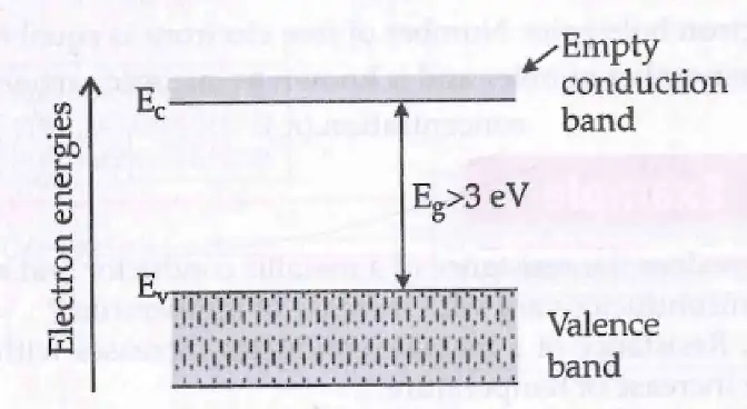
Insulators: Have a large energy gap (greater than 3 eV) between valence and conduction bands, preventing electrons from jumping to the conduction band, resulting in poor conductivity.
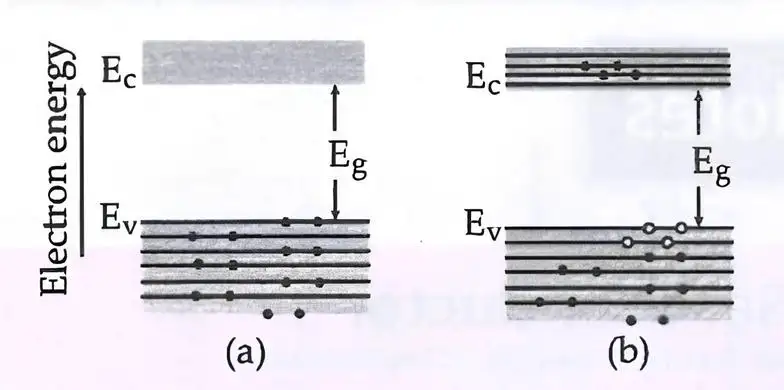
Semiconductors: Have a small energy gap (less than 3 eV). At room temperature, thermal energy can excite electrons from the valence band to the conduction band, enabling conduction.
Types of Semiconductors
Intrinsic Semiconductors: Pure semiconductors like silicon and germanium with equal numbers of free electrons and holes. Their conductivity is low and depends on temperature.
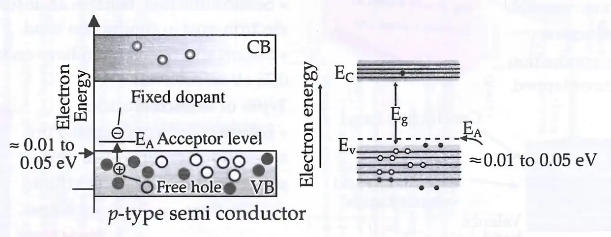
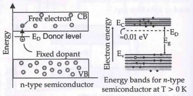
Extrinsic Semiconductors: Doped semiconductors with impurities added to increase conductivity.
- n-Type: Doped with pentavalent impurities (e.g., Antimony, Arsenic) that add extra electrons (majority carriers).
- p-Type: Doped with trivalent impurities (e.g., Boron, Gallium) that create holes (majority carriers).
Solved Examples
Example 1: How does the resistance of a metallic conductor and a semiconductor vary with increase of temperature?
Solution: The resistance of a metallic conductor increases with temperature because increased lattice vibrations hinder electron flow. In contrast, the resistance of a semiconductor decreases with temperature as more electrons gain enough energy to jump into the conduction band, increasing conductivity.
Practice Set
- Level 1 (Easy): Define the energy band gap in semiconductors.
- Level 2 (Moderate): Explain why semiconductors behave as insulators at absolute zero temperature.
- Level 3 (Challenging): Compare the energy band structures of conductors, semiconductors, and insulators and explain how these structures affect their electrical conductivity.
Answer Key
- Level 1: The energy band gap is the energy difference between the valence band and the conduction band in a material.
- Level 2: At absolute zero, semiconductors have no electrons in the conduction band because thermal energy is insufficient to excite electrons across the band gap, so they behave like insulators.
- Level 3: Conductors have overlapping valence and conduction bands allowing free electron movement; semiconductors have a small band gap allowing limited electron excitation; insulators have a large band gap preventing electron excitation, resulting in poor conductivity.
Semiconductor Diodes and Its Application
Semiconductor Diode Structure and Function
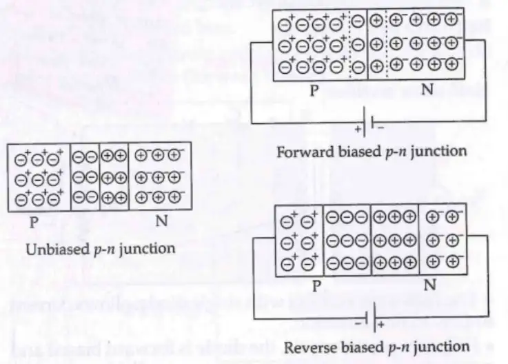
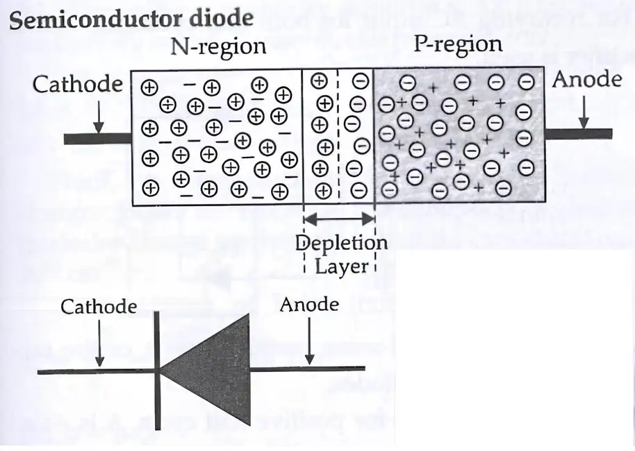
A semiconductor diode consists of a p-type and an n-type semiconductor joined together forming a p-n junction. The junction creates a depletion region that acts as a barrier to charge carrier movement.
Forward Bias: When the positive terminal of a battery is connected to the p-side and the negative to the n-side, the depletion region narrows, allowing current to flow easily.
Reverse Bias: When the positive terminal is connected to the n-side and the negative to the p-side, the depletion region widens, preventing current flow except for a small leakage current.
Diode Characteristics and Breakdown
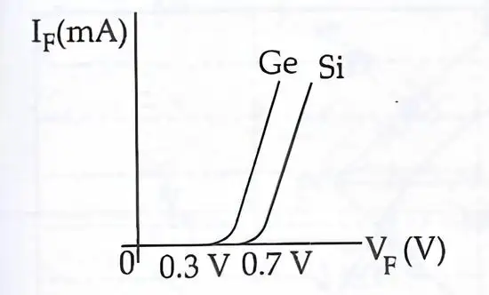
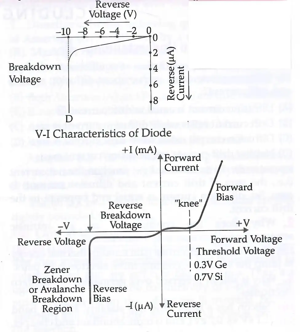
Diodes have a threshold voltage (about 0.7 V for silicon and 0.3 V for germanium) before they conduct in forward bias. In reverse bias, if the voltage exceeds a critical value, breakdown occurs via avalanche or Zener mechanisms, causing a large current.
Rectifiers
Rectifiers convert alternating current (AC) into direct current (DC).
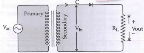
- Half-Wave Rectifier: Uses a single diode to allow only one half of the AC cycle to pass, producing pulsating DC.
- Full-Wave Rectifier: Uses two or four diodes and a center-tapped transformer to convert both halves of the AC cycle into pulsating DC.
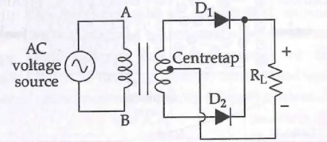
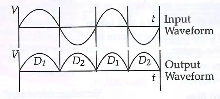
Solved Examples
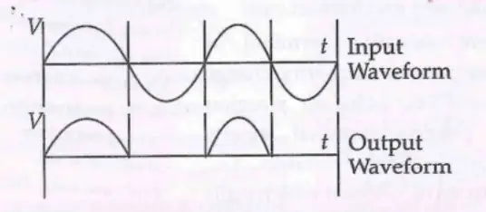
Example 1: Explain the working of a half-wave rectifier.
Solution: In a half-wave rectifier, during the positive half cycle of AC, the diode is forward biased and conducts current, allowing voltage across the load. During the negative half cycle, the diode is reverse biased and blocks current, resulting in no voltage across the load. The output is a pulsating DC voltage.
Practice Set
- Level 1 (Easy): What happens to the depletion region when a diode is forward biased?
- Level 2 (Moderate): Describe the difference in conduction between silicon and germanium diodes.
- Level 3 (Challenging): Explain the avalanche breakdown mechanism in a diode.
Answer Key
- Level 1: The depletion region narrows when the diode is forward biased, allowing current to flow.
- Level 2: Silicon diodes require about 0.7 V to conduct, while germanium diodes require about 0.3 V, making germanium diodes conduct at lower voltages.
- Level 3: Avalanche breakdown occurs when a high reverse voltage accelerates minority carriers, causing collisions that generate more carriers, rapidly increasing current.
Quick Reference Table
Energy Bands: Valence Band, Conduction Band, Forbidden Band (Energy Gap)
Material Types: Conductors (overlapping bands), Semiconductors (small gap < 3 eV), Insulators (large gap > 3 eV)
Semiconductor Types: Intrinsic (pure), Extrinsic (doped: n-type with pentavalent, p-type with trivalent impurities)
Diode Biasing: Forward Bias (depletion region narrows, current flows), Reverse Bias (depletion region widens, current blocked)
Rectifiers: Half-Wave (single diode), Full-Wave (two/four diodes with center-tapped transformer)
Common Mistakes and Misconceptions
- Confusing drift current with diffusion current in semiconductors.
- Believing that ions remain permanently on n-side or p-side after recombination; in reality, ions are immobile and the depletion region forms due to recombination.
- Incorrectly drawing circuit diagrams for rectifiers and diodes.
- Assuming semiconductors conduct at absolute zero; they behave as insulators at 0 K.
Glossary
- Depletion Region: The region around a p-n junction depleted of mobile charge carriers, acting as a barrier to current flow.
- Doping: The process of adding impurities to a semiconductor to change its electrical properties.
- Majority Carriers: The charge carriers (electrons or holes) present in the greatest number in a semiconductor.
- Minority Carriers: The charge carriers present in smaller numbers in a semiconductor.
- Rectifier: A device that converts alternating current (AC) to direct current (DC).
- Energy Band Gap: The energy difference between the valence band and conduction band in a material.