Fundamentals and Applications of Semiconductors
Charge Carriers and Their Movement in Semiconductors
Understanding Electrons and Holes as Current Carriers
Semiconductors conduct electricity through the movement of two types of charge carriers: electrons and holes. Electrons carry a negative charge, while holes represent the absence of an electron in the valence band and behave as positive charge carriers. Both have equal magnitude of charge but opposite polarity, enabling current flow within the material.
Electrons move in the conduction band, whereas holes move within the valence band. The mobility of electrons is generally higher than that of holes due to differences in their effective masses and scattering interactions within the crystal lattice.
When an electron gains enough energy to leave its position in the lattice, it creates a hole at its original site. This hole can be visualized as a positive charge carrier moving through the lattice. The stronger attraction of holes to the atomic nuclei results in their reduced mobility compared to electrons.
For example, in intrinsic silicon at room temperature (300 K), the electron mobility is approximately \(1500 \text{ cm}^2/\text{V·s}\), while hole mobility is about \(475 \text{ cm}^2/\text{V·s}\).
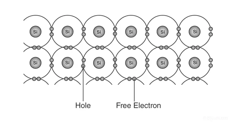
Visualization of electrons and holes in a semiconductor lattice
Example Problem
A silicon semiconductor at 300 K has electron mobility of \(1400 \text{ cm}^2/\text{V·s}\) and hole mobility of \(500 \text{ cm}^2/\text{V·s}\). Calculate the ratio of electron mobility to hole mobility.
Solution:
The ratio is given by:
\[ \frac{\mu_e}{\mu_h} = \frac{1400}{500} = 2.8 \]
This means electrons move approximately 2.8 times faster than holes in this silicon sample.
Energy Band Structure and Its Role in Semiconductors
Exploring Band Theory and Energy Levels
Band theory explains the electronic structure of solids by considering the splitting of atomic energy levels when atoms form a crystal lattice. Each atomic energy level broadens into a band of closely spaced levels in the solid. The two most important bands are the valence band, filled with electrons, and the conduction band, which is typically empty.
The energy gap between these bands, called the band gap, determines the electrical properties of the material. Semiconductors have a moderate band gap, allowing electrons to jump from the valence band to the conduction band when supplied with sufficient energy, such as heat or light.
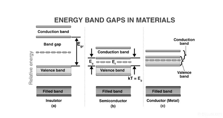
Energy band diagrams for different types of materials
The Fermi level, denoted as \(E_F\), lies between the valence and conduction bands and represents the highest occupied energy level at absolute zero temperature. At higher temperatures, electrons can occupy states above the Fermi level, enabling conduction.
Example Problem
Calculate the energy of a photon required to excite an electron across a semiconductor band gap of 1.2 eV. Also, find the corresponding wavelength of this photon.
Solution:
The energy \(E\) of the photon is equal to the band gap:
\[ E = 1.2 \text{ eV} = 1.2 \times 1.6 \times 10^{-19} \text{ J} = 1.92 \times 10^{-19} \text{ J} \]
The wavelength \(\lambda\) is given by:
\[ \lambda = \frac{hc}{E} = \frac{6.626 \times 10^{-34} \times 3 \times 10^{8}}{1.92 \times 10^{-19}} = 1.036 \times 10^{-6} \text{ m} = 1036 \text{ nm} \]
This wavelength lies in the infrared region of the electromagnetic spectrum.
Classification and Characteristics of Semiconductor Types
Intrinsic Semiconductors: Pure and Balanced Charge Carriers
Intrinsic semiconductors are composed of chemically pure materials, such as silicon or germanium, containing only one type of atom. At absolute zero, all electrons are bound in covalent bonds, and the material behaves as an insulator. As temperature increases, some electrons gain enough thermal energy to jump into the conduction band, leaving behind holes in the valence band.
In intrinsic semiconductors, the number of free electrons equals the number of holes, and both contribute equally to electrical conduction.
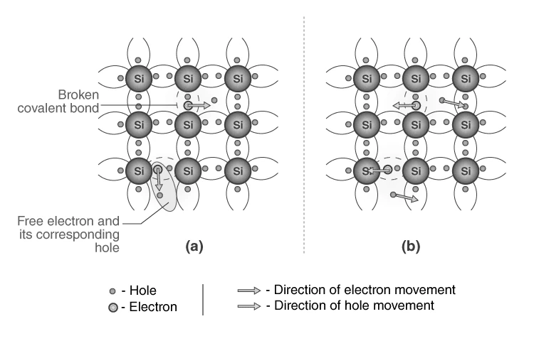
Electron and hole movement in intrinsic semiconductors
The total current \(I\) in intrinsic semiconductors is the sum of electron current \(I_e\) and hole current \(I_h\):
\[ I = I_e + I_h \]
The intrinsic carrier concentration \(n\) depends on the band gap \(E_g\), temperature \(T\), and Boltzmann constant \(k_B\) as:
\[ n = n_0 e^{-\frac{E_g}{2 k_B T}} \]
Extrinsic Semiconductors: Enhanced Conductivity through Doping
Extrinsic semiconductors are created by introducing small amounts of impurities into pure semiconductors, a process called doping. This significantly increases conductivity by adding extra charge carriers.
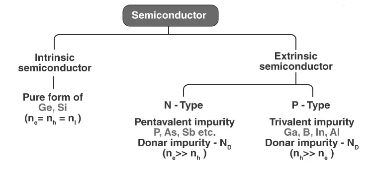
Types of semiconductors based on doping
N-Type Semiconductors
When pentavalent impurities (such as phosphorus or arsenic) are added, they donate extra electrons to the conduction band. These free electrons become the majority carriers, while holes are minority carriers. The crystal remains electrically neutral overall, with donor atoms becoming fixed positive ions.
P-Type Semiconductors
Doping with trivalent impurities (such as boron or gallium) creates holes by accepting electrons from the valence band. Holes become the majority carriers, and electrons are the minority carriers. The acceptor atoms become fixed negative ions, maintaining overall neutrality.
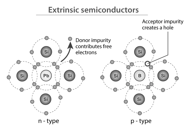
Doping effects in n-type and p-type semiconductors
Example Problem
A pure silicon sample is doped with a pentavalent impurity, increasing the free electron concentration to \(5 \times 10^{22} \text{ m}^{-3}\). If the hole concentration is \(1 \times 10^{10} \text{ m}^{-3}\), identify the type of semiconductor and state the majority carrier.
Solution:
Since the electron concentration \(n_e = 5 \times 10^{22} \text{ m}^{-3}\) is much greater than the hole concentration \(n_h = 1 \times 10^{10} \text{ m}^{-3}\), electrons are the majority carriers.
This indicates the semiconductor is n-type.
Practical Uses and Significance of Semiconductors
Everyday Applications of Semiconductor Materials
Semiconductors are integral to modern electronics due to their controlled conductivity and compact size. They are used in devices such as transistors, diodes, solar cells, and integrated circuits, enabling technologies like computers, smartphones, and sensors.
Examples include temperature sensors, microchips in autonomous vehicles, calculators, and 3D printers. Semiconductor switches like MOSFETs are essential components in electrical circuits.
Diverse applications of semiconductor devices
Industrial Importance and Advantages
Semiconductors enable the creation of advanced technologies such as LEDs, microprocessors, and solar panels. Their small size, low power consumption, durability, and noise-free operation make them indispensable in industrial and consumer electronics.
Key benefits include portability, energy efficiency, shock resistance, and long operational life.
Example Problem
Calculate the maximum wavelength of light that can excite an electron across the band gap of silicon, given \(E_g = 1.14 \text{ eV}\).
Solution:
Using the relation \(\lambda = \frac{hc}{E}\), where \(h = 6.626 \times 10^{-34} \text{ Js}\), \(c = 3 \times 10^{8} \text{ m/s}\), and \(E = 1.14 \times 1.6 \times 10^{-19} \text{ J}\):
\[ \lambda = \frac{6.626 \times 10^{-34} \times 3 \times 10^{8}}{1.14 \times 1.6 \times 10^{-19}} = 1.09 \times 10^{-6} \text{ m} = 10900 \text{ Å} \]
This wavelength corresponds to near-infrared light, which silicon can absorb to generate electron-hole pairs.
Quick Reference: Key Semiconductor Concepts
Concept | Description | Typical Values/Examples |
|---|---|---|
Intrinsic Semiconductor | Pure semiconductor with equal electrons and holes | Silicon, Germanium |
Extrinsic Semiconductor | Doped semiconductor with majority carriers | N-type (phosphorus-doped), P-type (boron-doped) |
Electron Mobility | Speed of electrons under electric field | ~1500 cm²/V·s (Si at 300 K) |
Hole Mobility | Speed of holes under electric field | ~475 cm²/V·s (Si at 300 K) |
Band Gap | Energy difference between valence and conduction bands | 1.12 eV (Silicon), 0.66 eV (Germanium) |
Fermi Level | Highest occupied energy level at 0 K | Between valence and conduction bands |
Doping | Adding impurities to modify conductivity | Donors (N-type), Acceptors (P-type) |
Majority Carriers | Dominant charge carriers in doped semiconductors | Electrons in N-type, Holes in P-type |
Minority Carriers | Less abundant charge carriers | Holes in N-type, Electrons in P-type |
Resistivity Temperature Coefficient | Change of resistivity with temperature | Negative for semiconductors |
Glossary of Semiconductor Terms
Term | Definition |
|---|---|
Band Gap | Energy difference between valence and conduction bands where no electron states exist |
Conduction Band | Energy band where electrons are free to move and conduct electricity |
Valence Band | Highest energy band filled with electrons at absolute zero |
Electron Mobility | Measure of how quickly electrons move through a semiconductor under an electric field |
Hole | Absence of an electron in the valence band acting as a positive charge carrier |
Doping | Process of adding impurities to a semiconductor to change its electrical properties |
Intrinsic Semiconductor | Pure semiconductor material without any significant impurities |
Extrinsic Semiconductor | Semiconductor with added impurities to increase conductivity |
Fermi Level | Energy level at which the probability of finding an electron is 50% at absolute zero |
Majority Carrier | Charge carrier present in the greatest concentration in a doped semiconductor |
Frequently Asked Questions
Why do semiconductors have a negative temperature coefficient of resistance?
As temperature rises, more electrons gain enough energy to jump into the conduction band, increasing charge carriers and decreasing resistivity, resulting in a negative temperature coefficient.
What distinguishes intrinsic from extrinsic semiconductors?
Intrinsic semiconductors are pure materials with equal electrons and holes, while extrinsic semiconductors are doped to increase either electron or hole concentration, enhancing conductivity.
How does doping affect the electrical properties of semiconductors?
Doping introduces impurities that add free electrons (n-type) or holes (p-type), significantly increasing the material's conductivity and enabling control over its electrical behavior.
What is the significance of the Fermi level in semiconductors?
The Fermi level indicates the energy level at which the probability of electron occupancy is 50% at absolute zero, influencing the distribution of electrons and holes at higher temperatures.
Why are electrons more mobile than holes in semiconductors?
Electrons have a smaller effective mass and experience less scattering than holes, allowing them to move more freely and with higher mobility within the crystal lattice.