Bipolar Junction Transistor: Structure, Operation, and Applications
Understanding the Bipolar Junction Transistor
Fundamentals and Symbol Representation
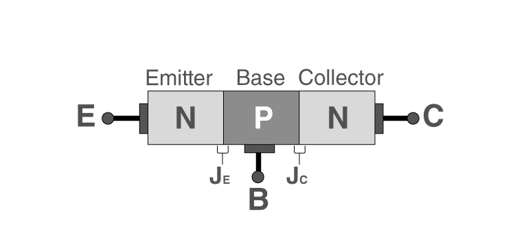
A Bipolar Junction Transistor (BJT) is a semiconductor device with three terminals: the emitter, base, and collector. It contains two p-n junctions and functions primarily as a current amplifier. A small input current at the base controls a larger current flowing between the collector and emitter, enabling signal amplification. This device requires an external DC power source to operate effectively.
Symbolic representation of a Bipolar Junction Transistor
Example Problem
In a BJT circuit, a base current of \(20 \mu A\) produces a collector current of \(2 mA\). Calculate the current gain (\( \beta \)) of the transistor.
Solution:
The current gain \( \beta \) is the ratio of collector current \( I_C \) to base current \( I_B \):
\[ \beta = \frac{I_C}{I_B} = \frac{2 \times 10^{-3} \text{ A}}{20 \times 10^{-6} \text{ A}} = 100 \]
Thus, the transistor amplifies the base current by a factor of 100.
Design and Working Principles of BJTs
Physical Construction and Types
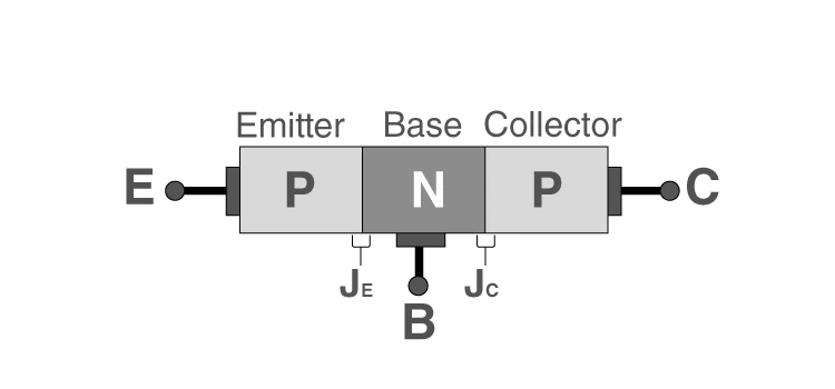
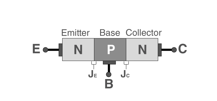
A BJT is built from three doped semiconductor regions: the emitter, base, and collector, separated by two p-n junctions. There are two main types of BJTs based on doping arrangement: NPN and PNP. In an NPN transistor, a p-type base is sandwiched between two n-type regions, while in a PNP transistor, an n-type base lies between two p-type regions. These configurations determine the direction of current flow and biasing requirements.
Cross-sectional view of a PNP Bipolar Junction Transistor
Cross-sectional view of an NPN Bipolar Junction Transistor
Example Problem
Identify the type of BJT if the emitter-base junction is forward biased with holes as majority carriers entering the base.
Solution:
Since holes are majority carriers entering the base, the emitter must be p-type and the base n-type, indicating a PNP transistor.
Modes of Operation and Regions
BJTs operate in three distinct regions depending on the biasing of the junctions:
Active Region: The transistor amplifies signals; the emitter-base junction is forward biased, and the collector-base junction is reverse biased.
Saturation Region: Both junctions are forward biased; the transistor acts as a closed switch with maximum collector current.
Cut-off Region: Both junctions are reverse biased; the transistor is off, and collector current is nearly zero.
Example Problem
A transistor has a collector current of \(5 mA\) when the base current is \(50 \mu A\). If the transistor is in saturation, what can be said about the collector-emitter voltage?
Solution:
In saturation, the transistor behaves like a closed switch, so the collector-emitter voltage \( V_{CE} \) is very low, typically around \(0.2 \text{ V}\), indicating the transistor is fully on.
Charge Dynamics, Configurations, and Practical Uses
Charge Flow and Voltage Control in BJTs
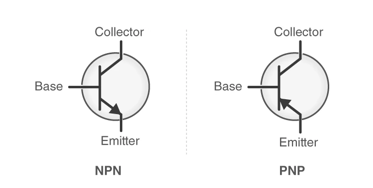
The operation of a BJT depends on the diffusion of charge carriers across the junctions. The emitter is heavily doped to inject a large number of carriers into the base, which is lightly doped and thin. The base-emitter junction is forward biased, allowing carrier injection, while the base-collector junction is reverse biased, collecting carriers. The collector current is controlled by the base current, and transistor models like the Gummel-Poon model describe this charge distribution and current flow.
Charge carrier movement in NPN and PNP transistors
Example Problem
Explain why the emitter is doped more heavily than the base in a BJT.
Solution:
The emitter must supply a large number of charge carriers to the base.
Heavy doping increases carrier concentration, enhancing injection efficiency.
The base is lightly doped to allow most carriers to diffuse through to the collector.
Common Connection Configurations and Their Characteristics
BJTs can be connected in three standard configurations, each with unique input-output relationships:
Common Emitter (CE): Provides both voltage and current gain; widely used in amplification circuits.
Common Collector (CC): Also called an emitter follower; offers current gain but no voltage gain.
Common Base (CB): Provides voltage gain but no current gain; used in high-frequency applications.
Configuration | Voltage Gain | Current Gain | Typical Use |
|---|---|---|---|
Common Emitter | High | High | Amplifiers |
Common Collector | Approximately 1 | High | Impedance matching |
Common Base | High | Approximately 1 | High-frequency circuits |
Example Problem
Which BJT configuration would you choose for a voltage amplifier circuit requiring high voltage gain and why?
Solution:
The common emitter configuration is ideal because it provides both high voltage and current gain, making it suitable for voltage amplification.
Practical Applications of Bipolar Junction Transistors
BJTs are versatile components used in various electronic devices. Their ability to amplify and switch currents makes them essential in:
Amplifiers in audio and radio frequency circuits
Switching devices in digital logic circuits
Oscillators generating periodic signals
Demodulators for extracting information from modulated signals
Wave shaping circuits such as clippers
Example Problem
Describe two applications of BJTs in communication devices.
Solution:
Used as amplifiers to boost weak radio signals for clear reception.
Employed as demodulators to extract audio signals from modulated carrier waves.
Quick Reference Summary
Aspect | Details |
|---|---|
Inventors | W. Shockley, J. Bardeen, W. Brattain (1947) |
Terminals | Emitter, Base, Collector |
Types | NPN and PNP |
Operating Regions | Active, Saturation, Cut-off |
Common Configurations | Common Emitter, Common Collector, Common Base |
Primary Function | Current amplification and switching |
Applications | Amplifiers, switches, oscillators, demodulators |
Biasing | Base-emitter junction forward biased; base-collector junction reverse biased in active mode |
Current Gain (\( \beta \)) | Ratio of collector current to base current |
Voltage Gain | High in common emitter and common base configurations |
Glossary of Key Terms
Term | Definition |
|---|---|
Bipolar Junction Transistor (BJT) | A semiconductor device with two p-n junctions used for amplification and switching. |
Emitter | The terminal that emits charge carriers into the base. |
Base | The thin, lightly doped middle region controlling transistor operation. |
Collector | The terminal that collects carriers from the base region. |
Forward Bias | Condition where the p-n junction allows current flow. |
Reverse Bias | Condition where the p-n junction blocks current flow. |
Current Gain (\( \beta \)) | The ratio of collector current to base current in a BJT. |
Active Region | Operating mode where the transistor amplifies signals. |
Saturation Region | Mode where the transistor is fully on, acting as a closed switch. |
Cut-off Region | Mode where the transistor is off, with no collector current. |
Frequently Asked Questions
Who were the inventors of the Bipolar Junction Transistor?
The BJT was developed in 1947 by William Shockley, John Bardeen, and Walter Brattain.
What are the main operating regions of a BJT?
The three primary regions are active (amplification), saturation (fully on), and cut-off (fully off).
What are common uses of BJTs in electronics?
BJTs are widely used as amplifiers, switches, oscillators, and demodulators in various circuits.
What happens if a BJT is not properly biased?
Improper biasing can cause reduced efficiency, signal distortion, shifting of operating point, and altered transistor parameters.
Why is there a maximum voltage limit on the collector supply?
Exceeding the maximum collector voltage can damage the transistor due to excessive current and heat generation.